PCB Design
Individual Subsystem PCB Design
This page contains all design files and documentation for the ESP32 Wireless Communication Subsystem, including the PCB layout. The system integrates an ESP32-S3-WROOM-1-N8R8 Wi-Fi module, OV5640 camera module, AP63203WU-7 buck regulator, debug LEDs, tactile switches, and supporting circuitry for wireless communication and image capture.
ECAD Layer Views
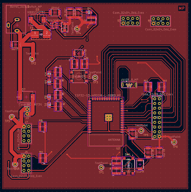
Figure 01: PCB Top Layer View (ECAD)
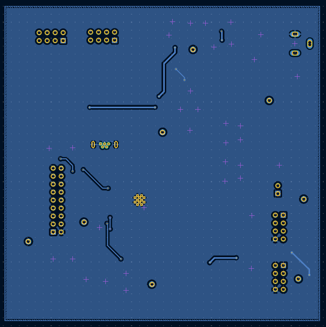
Figure 02: PCB Bottom Layer View (ECAD)
Physical PCB Photos
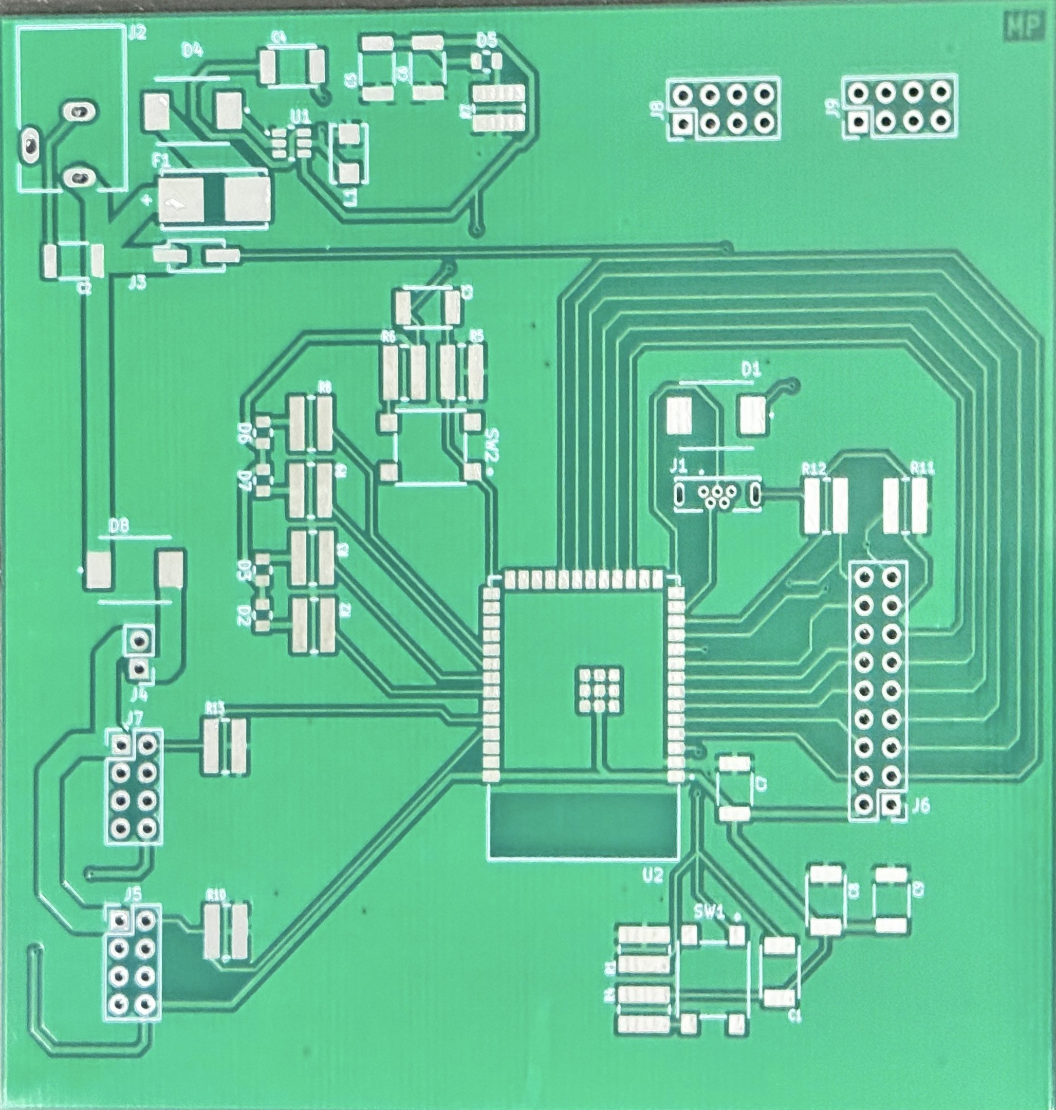
Figure 03: Raw PCB Before Population (before soldering)
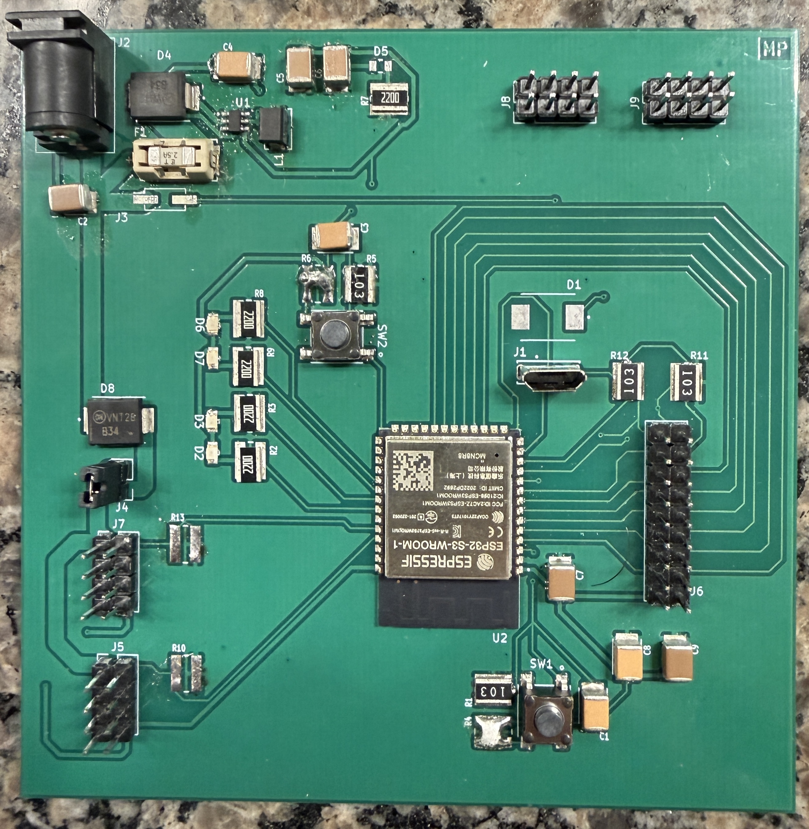
Figure 04: Finalized PCB After Soldering and Testing
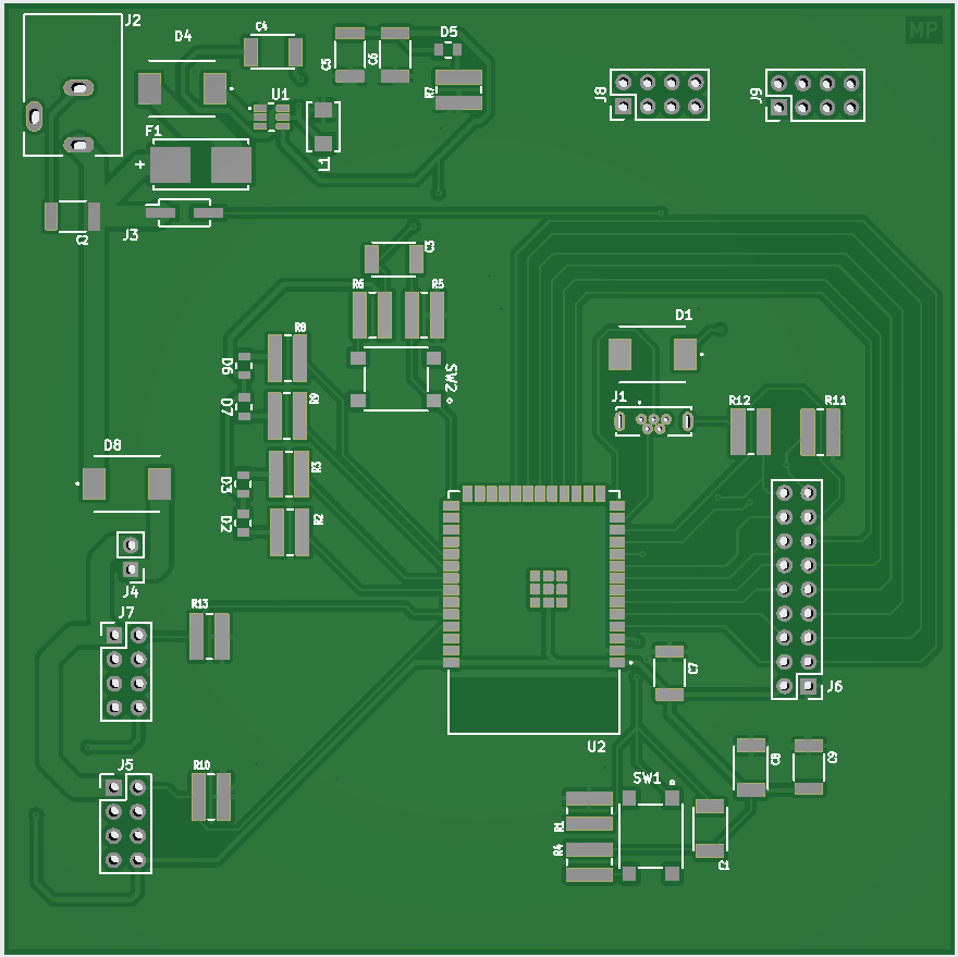
Figure 05: PCB Front View (populated)
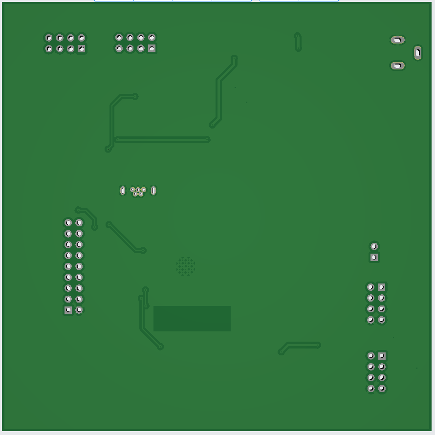
Figure 06: PCB Back View (populated)
Downloadable Files
-
Project ZIP:
Download KiCad Project ZIP -
PCB Gerber Files ZIP:
Download PCB Gerber Files ZIP -
PCB Footprints Library ZIP:
Download PCB Footprints Library ZIP -
PCB PDF:
Wireless Communication PCB PDF -
PCB Top Layer Image:
Wireless Communication PCB Top Layer Image -
PCB Top Layer PDF:
Wireless Communication PCB Top Layer PDF -
PCB Bottom Layer Image:
Wireless Communication PCB Bottom Layer Image -
PCB Bottom Layer PDF:
Wireless Communication PCB Bottom Layer PDF